Harry Tuller wins Egleston Medal for his electroceramics work
- Post by: Tuller Group
- May 3, 2019
- Comments off
Pioneering materials science and engineering research enables better catalytic converters, miniature explosives detectors, and thin-film microbalances.
What do catalytic converters, miniature explosives detectors, and scales for weighing nanoscale quantities have in common? These technologies are all enabled by MIT Professor Harry L. Tuller’s pioneering research on electroceramics, which are complex materials that exhibit a distinctive variety of electrical, optical, magnetic, ionic, and electronic properties.
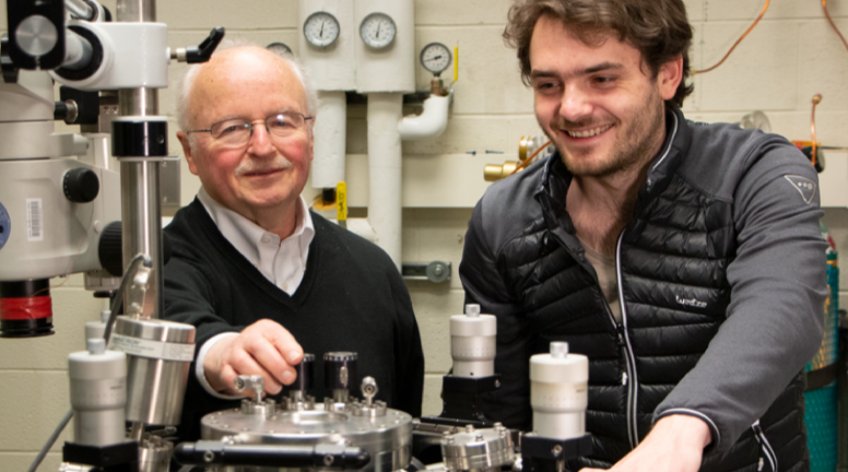
Photo: Denis Paiste/MIT Materials Research Laboratory
In more than 40 years on the MIT Department of Materials Science and Engineering faculty, Tuller also has mentored many graduate students and postdocs, edited a specialized ceramics journal, and co-founded Boston MicroSystems, based on applications of his breakthrough method for micromachining silicon carbide. His work most often focuses on materials that can operate at high temperatures — for example, in fuel cells and auto exhaust manifolds.
This spring, Tuller, 74, will receive for his accomplishments the Thomas Egleston Medal from his alma mater, Columbia University, where he earned both undergraduate and graduate degrees in electrical engineering and a doctorate in solid-state science and engineering.
“I am truly happy to hear that Prof. Tuller will be honored with the Egleston Medal,” says Il-Doo Kim, professor of materials science and engineering at the Korea Advanced Institute of Science and Technology (KAIST) in the Republic of Korea. Kim worked at MIT as a postdoc in Tuller’s Crystal Physics and Electroceramics Laboratory from 2003 to 2005, and he continues to collaborate with Tuller on research.
“As the editor-in-chief of the Journal of Electroceramics (since 1997) and a world-leading scientist, Prof. Tuller has accomplished a vast number of fascinating high-impact works that contributed significantly to the fields of electroceramics and solid state ionics; that is, defects, electronic structure, and transport of metal oxides and their integration into sensors and fuel cells,” Kim adds. Tuller served as president of the International Society of Solid State Ionics from 2015 to 2017.
Faculty mentor
MIT Professor Bilge Yildiz, who teaches in both the departments of Nuclear Science and Engineering and Materials Science and Engineering, says she is grateful to Tuller for mentoring her through her own tenure track at MIT, and for their continued collaboration. “Professor Tuller is the giant, the most significant figure in the advancement of electroceramics that are enablers to many important technologies, including energy conversion and storage, communications, electronics, and sensing. Because his work is so fundamental and based on physical principles, his contributions cross-cut and advance all of these wide-ranging applications,” Yildiz notes. Yildiz, Tuller, and three international collaborators won the International Union of Materials Research Societies Somiya Award in 2012 for their work on designing ionic and mixed conducting ceramics for fuel cells.
Avner Rothschild, now a professor of Electrochemical Materials and Devices in the Department of Materials Science and Engineering at the Technion – Israel Institute of Technology in Haifa, Israel, served as a postdoc under Tuller from 2003 to 2006. “I will always remember the years I spent with Harry Tuller as the most exciting time in my professional career,” Rothschild says.
“Many technologies rely on our ability to tailor the electronic and ionic conductivities in ceramic materials, so-called electroceramic materials. For instance, the combustion process in our cars is controlled by oxygen sensors made of zirconium oxide (ZrO2), and toxic exhaust gases such as carbon monoxide (CO) and nitric oxide (NO) are converted to benign gases such as carbon dioxide (CO2), nitrogen (N2) and oxygen (O2) in the catalytic converter that is made of cerium oxide (CeO2),” Rothschild notes.
Enabling nanoionics
Tuller pioneered the defect chemistry and ionic transport in cerium oxide, an important material in catalytic converters, gas sensors, and fuel cells, while still a graduate student at Columbia University, Rothschild points out. “His doctoral work in Columbia University laid the foundation for understanding how doping — that is, substituting a tiny fraction of one of the constituent elements in an ionic compound with another element — modifies its electrical properties and opens up the way to create new functional materials with tailored electronic and ionic conductivities,” Rothschild says. “For two generations, Harry Tuller has been and continues to be the main authority in the field of defect chemistry and ionic and electronic transport in solid-state ionic materials and devices. His research encompasses a vast variety of materials, devices, and phenomena, making landmark contributions in many different areas within this field. For example, he pioneered the defect chemistry and ionic transport in nanocrystalline materials, paving the road to a new area of research called nanoionics.”
Tuller’s work is known for its creativity, scientific depth, and analytical precision, Rothschild says. Tuller has published more than 480 articles, co-edited 15 books, and been awarded 34 patents. The Thomas Egleston Medal for Distinguished Engineering Achievement, awarded annually since 1939, is named for a key founder of the Columbia College School of Mines, which grew into today’s Fu Foundation School of Engineering and Applied Science at Columbia University. Tuller will receive the award in New York City on May 30.
Micromachining silicon carbide
Among his many accomplishments, Tuller says the most exciting was the research developing a micromachining process for diamond-like silicon carbide and shepherding it from lab bench to startup firm Boston MicroSystems through that firm’s acquisition by Pall Corp. in 2013. “This was kind of a fantastic opportunity to start from very fundamental questions in the laboratory, formulate ideas for patents, which were then developed at MIT, and demonstrate that yes, these concepts can be translated into technological innovations, and that they are practical,” Tuller explains.
Tuller’s research in this area was motivated by some fundamental limits of important high-tech materials such as silicon, commonly used for computer chips because of its ability, in the form of p-n junctions, to switch between states that block or transmit electrical signals (insulating and conductive states); and quartz, used for wristwatches because of its ability to expand or contract in response to an electrical signal (piezoelectric response) and be driven to resonate. Neither material could stand up to the high-temperature environments for which Tuller sought to develop similar applications, such as specialized micro-electro-mechanical devices (MEMS). Such MEMS devices tell a car’s airbag when to turn on, for example, but MEMS have been developed for a wide range of applications, from gyroscopes in airplanes to laboratories on a chip.
Silicon loses its semiconducting ability at about 150 degrees Celsius (about 300 degrees Fahrenheit) and it loses its mechanical strength at about 400 C (about 750 F), Tuller explains. At about 400-500 C, quartz undergoes a destructive transformation in its crystal structure that causes it to shatter. “We discovered a class of very high-temperature piezoelectric materials, that we’ve been refining over a period of years, and now we can replicate at 1,000 degrees Celsius the same level of performance that you can achieve at room temperature,” Tuller says.
“The problem with something which is diamond-like is that it is resistant to nearly every kind of chemical that you could imagine,” Tuller says. “So if you attempt to apply a similar chemical etching route as used in silicon to remove material on an atomic scale, it becomes nearly impossible.” Tuller, and then-MIT graduate student Richard F. Mlcak ScD ’94 developed a process to micromachine silicon carbide, which is much closer to diamond than to silicon in its ability to withstand high temperatures and retain its semiconducting properties. “So now, suddenly we could essentially replicate everything people could do in silicon in silicon carbide,” Tuller explains.
“And it turns out coincidentally, bringing those two different fields together, that there is a very similar compound to silicon carbide in terms of its crystal structure and lattice parameter and properties, called gallium nitride, which happens to be piezoelectric. So actually, we’re able to do something which was quite unique, and that is to apply thin layers of gallium nitride to silicon carbide, and thereby cause those MEMS structures to vibrate in a similar way as the quartz crystal monitor, except on a very tiny scale. So now we’re able to make these piezoelectric resonators, working at 10 megahertz, on structures just hundreds of microns in dimensions. We combined those two technologies to form arrays of these sensors and, under support from Homeland Security Agency and NASA, we developed a series of devices which could detect explosives and toxic chemicals,” he says. Remarkably, the new MEMS-based sensor, which occupies a chip just a few millimeters in size (about one-eighth inch) can replace large benchtop devices like mass spectrometers that cost about $50,000 each. It became the basis for Boston Microsystems, a pioneer in MEMS designed for harsh environments, and high-sensitivity sensors for use in explosives detection and industrial monitoring.
Making connections
The ups and downs of that process enriched his interactions with students, Tuller says. “Something I like about being at MIT is that we’re interested in the connection between fundamental issues and engineering applications. And, I think, to be a good educator at a place like MIT, you have to be able to make those connections, and it’s hard to make those connections unless you’ve had actual experience in the field.”
Taking a new process from laboratory to market means having to deal not just with technical issues, but also with economic issues, Tuller says. “Can you do this in a cost-effective manner? Are there customers who are going to be interested in your product? Can it be manufactured at scale? So suddenly, you have to address all these practical issues and, I think, having gone through that process, which sometimes is very painful, I come back in the laboratory, and I think that I can now do a much better job of making those connections for the students,” Tuller says. “And I think that’s one of the things that attracts a lot of students to MIT. It’s not just theory and science, but they know that there are people here who have that excitement about science translated into practice.” In April 2018, Tuller received the Committed to Caring Award at MIT, for which he was nominated by several of his own students.
Electronic nose
Former students and postdocs in Tuller’s group have gone on to positions at top universities and research institutes in Austria, Finland, France, Germany, India, Israel, Japan, Korea, and Switzerland. Former Tuller doctoral student Woochul Jung PhD ’10, participated in the development of an “electronic nose” in Tuller’s lab and is now an associate professor of Materials Science and Engineering at KAIST. “Professor Tuller is an excellent mentor who always encourages people around him with endless passion and intellectual curiosity,” Jung says. “Above all, he showed me the life of a scientist who enjoys the journey of asking questions and logically finding answers, which has been the most important teaching in my academic career so far.”
Tuller is collaborating with his former postdoc Il-Doo Kim at KAIST on extending the “electronic nose” technology to health monitoring. “Here you would just have someone breathe into your device and it would electronically tell you that this person likely has a particular disease: diabetes, or malaria, or even certain kinds of cancer,” Tuller says.
Tuller is now probing how to use color differences as a measurement tool for monitoring defect creation/annihilation and the efficiency of fuel cell electrodes. “A particular material that we’re very much interested in now as a fuel cell electrode is praseodymium cerium oxide. And it turns out, this material under normal conditions is quite a deep red. But as we reduce the oxygen content of the gas phase, it becomes less and less intense red until it becomes transparent. And it turns out over that fairly wide range of gas composition, the intensity of that red can be correlated with the defects, the number of defects, in this material which control its properties,” Tuller says. By monitoring the rate of change in color following a step change in gas composition, one can also characterize the efficiency of the fuel cell electrode and its longer-term degradation.
In 2018, the U.S. Department of Energy renewed funding for the Chemomechanics of Far-From-Equilibrium Interfaces (COFFEI) research project, which was its fourth three-year award. The COFFEI program, a collaboration with five other MIT colleagues, couples chemical and mechanical behavior of electroceramic oxides. Tuller also actively participated in MIT-Skoltech Center for Electrochemical Energy Storage.
Exploiting defects
Defects in an electroceramic material lead to nearly all of its interesting functional properties, whether electronic, optical, or magnetic. In energy storage and conversion systems such as batteries and fuel cells, it is the migration of ions that confers on them their electrical properties. “For lithium batteries, it’s lithium ions. For fuel cell materials, it’s usually oxygen or hydrogen ions — protons — that are mobile, and all of those defects are within the crystal lattice,” Tuller explains. “That’s what allows them to actually transport matter, while the electronic properties also depend on the creation of defects in the structure.”
“So being able to identify, monitor and predict how the defect concentrations will depend on the composition of the material, impurities, microstructure, temperature, atmosphere are all critical in being able to predict and optimize the properties of those materials,” he says. “And that’s something that we spent a lot of time trying to formalize, develop methods to improve characterization and also to model the connection between the defects and the properties of interest in specific applications.” The pico-level microbalances that Tuller developed can detect quantities as tiny as trillionths of a gram.
That quest for structure and order in materials carries over into Tuller’s personal hobbies, which include classic sports cars, gardening, and photography. He has been a car buff since his college days, and last fall Tuller began restoring a 1972 Jaguar XKE, which he calls one of the most beautiful vehicles ever built. With his research frequently taking him to Japan, Tuller has developed an interest in Japanese gardens. His photography focuses on scenery or architecture. “It’s about form and function, that is what engineering is all about. The same thing as with gardening, the form and the function. There’s something to that,” he says.
Tuller and his wife, Sonia, live in Wellesley, Massachusetts. They have two adult daughters, who also live in greater Boston with their spouses, and three grandchildren.
Tuller has served on the MIT faculty, since 1975, after completing his doctorate at Columbia and a postdoc at the Technion – Israel Institute of Technology. “I’ve loved being at MIT all these years; it’s actually my first permanent job. The thing I love about MIT is what a stimulating environment it is; but at times I have to limit myself, because it easily becomes overstimulating,” Tuller says.